Quantitative Measurements of FPGA Utility in
Special and General Purpose Processors
Barry S. Fagin
Thayer School of Engineering
Dartmouth College
Hanover, NH
03755
603-646-3060
barry.fagin@dartmouth.edu
ABSTRACT
We present experimental results on FPGA use in
special and general purpose processors, using as case studies a computational
accelerator for gene sequence analysis,
an integer implementation of the DLX microprocessor, and a real-time
signal processor for rocket telemetry.
All these devices have been successfully prototyped, and are now
completely functional. We present
detailed analysis of our experience with FPGAs in these machines, describing
savings in chip count, power consumption, area, and cost. For all quantities
except cost, measured savings were typically an order of magnitude improvement
over discrete IC implementations.
1.0 Introduction
Recent work at the Thayer School of
Engineering has investigated the use of FPGAs in a variety of digital
systems. We present here our results on
FPGA usage in three advanced designs: a special purpose processor for gene
sequence analysis, known as the GSP, an implementation of Patterson and
Hennessy's DLX 32-bit microprocessor architecture, and a real-time signal
processor for rocket telemetry know as the Plasma Frequency Tracker.
We first provide an overview of the
laboratory where these machines were constructed, and then give an overview of
the three processors. Architectural
tradeoffs concerning the use of FPGAs are discussed. We then present our
quantitative data and analyze it in detail. We compare our results in light of
the special purpose and general purpose nature of the respective designs, and
note similarities and differences.
Finally, we offer our conclusions on the utility of FPGAs for processor design.
Throughout this paper we assume the
reader is familiar with field programmable gate arrays. For background information on the devices
used, the reader is referred to [1] and [2].
2.0 The Thayer Rapid Prototyping Facility
The systems described here were built
at the Thayer Rapid Prototyping Facility, a laboratory for the rapid
construction and evaluation of digital systems.
The RPF emphasizes in-house prototype development using semi-custom
ASICs and printed circuit boards to avoid the lengthy turnaround time of a
VLSI-based approach. This approach uses
a new printing technology developed by Direct Imaging Inc. to produce PCB's
in-house, supporting 5 mil traces at 5 mil spacing, with up to 8 trace layers.
The goal of the RPF is to use this technology to produce prototypes as quickly
as possible.
The RPF has been involved in several
successful experiments in rapid digital system design. In addition to GSP, DLX, and the Plasma
Frequency Tracker, other systems include an FHT transform engine and a hardware
monitor for the 68000. For further
information on these and other projects, the reader is referred to references
[3] through [8]. All projects described in this paper have been prototyped and
are fully functional.
3.0 The Processors
To better understand the use of FPGAs
in our designs, we give brief overviews of each of the systems under
study. The GSP and the Plasma Frequency
Tracker are special purpose devices, while DLX is a general purpose 32-bit
microprocessor.
3.1 The Gene Sequence Processor
One of the more recent systems to be
prototyped at the RPF is the Gene Sequence Processor, a computational
accelerator for gene sequence comparison.
The GSP consists of two boards that connect to the NuBus slots of a Mac
II f/x computer, increasing its performance by 15x for certain problems. Gene sequence comparison is essentially a
dynamic programming algorithm with a particularly defined cost function. The GSP contains extra memory and special
hardware to support the fast execution of DP algorithms with these functions on
sequences of nucleotides. For more
information on gene sequence comparison, the reader is referred to [9].
A block diagram of the Gene Sequence
Processor is shown in Figure 1. The GSP
consists of five basic subsystems: DRAM, SRAM, a counter/comparator, the host
interface, and the Gene ALU.
The GSP contains 8 megabytes of DRAM,
organized as a 4M x 16-bit words. The
DRAM holds the dynamic programming array for the alignment
computation. The sequences to be
compared, cost function coefficients, and sequence lengths are downloaded into
a 4k x 8 SRAM. The counter/comparator is
used to generate DRAM addresses for the dynamic
programming calculation, and to halt the computation when the last entry in the
dynamic programming array has been calculated.
The processor interface is responsible for all interaction with the
host. Currently, this interface is
implemented with TI NuBus chips, although general interfaces can be designed to
interact with a variety of hosts.
3.2
The Plasma Frequency Tracker
The Plasma Frequency Tracker, or PFT,
is one of several instruments scheduled
to go on board a NASA rocket flight in January 1993. Its primary purpose is to detect the presence
of Langmuir solitons, high energy events in the ionospheric plasma. The PFT consists of three boards: an onboard
computer, an interface board, and the output board. The onboard computer is a dedicated Q88/B
microprocessor used for data acquisition and analysis. The interface board handles data format
conversion between the rocket-borne experiment and the microprocessor, and
consists primarily of an Altera EPLD and an AD575 analog to digital
converter. The output board contains
four Actel FPGAs, a 12-bit A/D converter, and some analog circuitry. For our purposes, the most interesting part
of the output board is the Soliton Detector.
A block diagram of this subsystem is shown in Figure 2.
The Soliton Detector receives data from
two sources: a radio receiver, and a companion instrument that calculates
plasma resonance frequencies. Data from
the radio receiver goes through a 12-bit A/D converter and is converted to
signed magnitude representation. The
Master Counter is a 20-bit counter used for grouping data, along with the
Counter Register Bank, a 10 x 20-bit FIFO.
The Data Register Bank is a 19 x 12-bit FIFO used in conjunction with
the Window Detector and the Length Generator to implement the soliton detection
algorithm. Soliton events are indicated
by large changes in the plasma electric field, typically about 60dB greater
than background emissions. These changes
can be distinguished from noise by their bipolar nature; true soliton events
will have both positive and negative magnitude changes. Thus soliton detection is accomplished by
first examining the most significant 4 magnitude bits of the sampled data. If any of these bits are non-zero, a 1 is shifted
in to one of two 19-bit shift registers, depending on the sign of the
sample. If at any time both shift
registers contain a 1, the beginning of a soliton event has been detected.
(Soliton events have typical durations of several milliseconds; the PFT system
is designed to record the entire event). This triggers a change in the gain
state of the experiment, to accommodate the increased magnitude of the electric
field, and sends the appropriate information to the router. The router coordinates multiple inputs and
hands them off to the Altera EP1900 on the interface board for output format
conversion.
While the output format conversion
could have been handled by an Actel FPGA similar to those employed elsewhere,
an EP1900 was employed for reasons of speed and expandability. Although EPLD's do not offer the integration
of FPGA's, they are considerably faster.
The parallel-to-serial conversion performed by the output converter
requires output bit rates 12 times faster than input, placing severe
performance constraints on the selected technology. While the current sampling rate specified by
the telemetry experiment is within the limits of existing FPGA technology,
factor increases of 2 or 4 are not. To accommodate possible rate changes in
future experiments, therefore, we decided to employ a smaller and faster EPLD.
For more information on the Plasma
Frequency Tracker, the reader is referred to [6].
3.3
The DLX Microprocessor
For our case study in general purpose
processor implementation, we selected the DLX microprocessor. The DLX
is a 32-bit CPU, described in detail in [10]. This architecture is emerging as a standard
machine to illustrate basic RISC principles.
For readers unfamiliar with DLX, we give a brief overview here.
DLX is a complete microprocessor
architecture, with 32 general purpose registers and a hard-wired zero in
R0. Memory is Big Endian byte
addressable, and all instruction accesses are aligned. The integer DLX integer instruction set has three basic classes: data
transfer, arithmetic/logical, and control flow. (A floating point extension of
DLX is described in [10], which we did not implement). The DLX instruction set is highly
streamlined; the number of instructions and instruction formats is small, and
instruction decoding is simple.
A block diagram of the Thayer DLX
datapath is shown in Figure 3. The
Thayer DLX employs a 2-bus architecture, driven by a 32 x 32 register file, a
32-bit ALU, 32K of static ram, and a so-called "universal unit", or
UU. (A 32-bit instruction register,
IR, holds the current instruction). We chose a 2-bus architecture for three
reasons: 1) to match our available
register files, which shared input and output pins, 2) to improve the
routability of the board, and 3) to simplify the machine. This decision reflects a consistent
willingness to tradeoff performance for the increased likelihood of producing a
working prototype under time constraints. For more details about this and other
design decisions regarding the prototyping of DLX, the reader is referred to
[4]. We discuss the Universal Unit in
the next section.
4.0 FPGA Usage
The GSP, PFT, and DLX processors all
make use of FPGAs to implement various design subsystems. The GSP employs five devices to implement all
non-memory subsystems, the PFT uses four, while DLX employs one. FPGA utilization in each of these processors
is shown in Table 1. The name of the
FPGA in the design is given, along with its functionality and the device
chosen.
We chose the Actel family of FPGAs for
a number of reasons. Our initial
experiences with routing software indicated that placement and routing of
designs would be very easy on Actel parts.
Additionally, the PFT was designed as a rocket payload, an environment
well suited to non-volatile write-once devices.
Finally, for this study we wanted to keep the device family constant
across implementations to prevent technology-related effects from biasing the
results.
All our systems employed the ACT1
series of FPGAs. Some of these devices
are available with different pin counts and routing resources, as shown in
Table 2. The part number of each device
appears in column 1; the last two digits indicate the number of pins (not all
of which are available to the user). All
the devices we used were packaged in Plastic Leadless Chip Carriers, or PLCC's.
Actel FPGAs contain two principal
resources: logic blocks for user circuitry and i/o blocks for pins. The total
number of these blocks for each device appears in the second and third columns
of Table 2. The area of each device in
square inches appears in the next column, followed by the cost. Resource and area information are taken from
[1]. Cost figures are for small
quantities, obtained from our Actel distributor in April 1992.
4.1
FPGAs in the GSP
FPGA utilization in the GSP is shown in
the first section of Table 3. The GSP
employs five Actel devices: three 1020's and two 1010's.
We see from Table 1 that the GSP
required very little glue logic: most of the logical subsystems of the GSP
proved implementable with FPGAs.
Comparing Figure 1, we see that the 16-bit Gene ALU was successfully bit
sliced into two bytes, each using one 1020 FPGA, while another 1020 implemented
the counter/comparator subsystem. The
larger of the 1010's served as the
interface to the SRAM, while the smaller was used for a 10-bit 2-1 mux. This device is the only one that could have
conceivably been replaced with its TTL equivalents. The remaining subsystems of Figure 1 are
either RAM modules or the host interface.
This latter component was implemented with standard NuBus chips, as
their seemed little be gained from reimplementing an existing commercial
product.
We note that since FPGAs are used for
the basic comparison, other algorithms can be implemented by simply replacing
the "actelbi4" parts with other FPGAs, or by using reprogrammable
parts and reconfiguring them dynamically.
We are investigating this as a topic for future research.
4.2
FPGAs in the PFT
FPGA utilization in the PFT is shown in
the second section of Table 3. Only a
single FPGA device type is employed; all FPGA's in the PFT are ACT1020-68's.
Like the GSP, the PFT was able to utilize
FPGA's quite successfully. Virtually all
the logic on the output board was implemented with FPGA's; due to space constraints on the rocket payload, the
device literally could not have been built without them. The FPGA "dagc_contl" is used for
the control section of the board; it contains the sign converter, window
detector, length generator, and router.
"master3a" holds the master 20-bit counter on the board, along
with some related interface logic.
"cntrega" holds the counter register bank, while
"regbank" holds the data register bank.
4.3
FPGAs in DLX
Unlike the special purpose machines,
the DLX was able to employ only a single FPGA, due to the increased complexity
of its component subsytems. Referring to
Figure 3, we see that DLX, like most general purpose microprocessors, required
a 32-bit register file and an ALU. Both of these components were sufficiently
complex as to make FPGA implementation difficult. Additionally, these subsystems could be
implemented with a small number of low cost commercial ICs, negating much of
the chip count reduction advantage of FPGA implementation.
We found, however, that the Universal
Unit of Figure 3 was an attractive target for FPGA implementation. The UU is implemented with an Actel1020 FPGA,
initially adopted to implement a 32-bit barrel shifter. As the design progressed, we discovered that
more and more logic could be added to it
without increasing chip count or power consumption. Thus the shifter became the UU, containing
both the nontrivial sign-extension logic required by the DLX instruction set
and the memory alignment circuitry. The
ability to incorporate new logic into our design quickly and easily was crucial
to its success; the use of a field programmable gate array was absolutely
essential.
5.0 Empirical Measurements
We have analyzed the utility of each of
the 9 FPGAs described in Table 1, and discuss our results here. We present measurements on IC equivalent chip
count, pin count, area, power, and cost, along with measurements of logic and
i/o utilization for each device.
IC equivalence measurements are shown
in Table 3. All IC information is taken
from [11] and [12], while FPGA data was obtained from [1]. We describe each column of Table 3 below.
Chip
count: We have estimated the
equivalent number of discrete IC's replaced by an FPGA by going through the
schematic and mapping the design onto discrete components. This process is approximate, in that a design
specifically targeted for discrete IC's can differ in subtle ways from an FPGA
implementation. Designs for FPGAs will
be influenced by the items in the FPGA macro library, which may differ from the
IC's listed in a databook. Logic
polarities may be changed, and parts of the design that are highly tuned to a
particular FPGA macro could change substantially if implemented in discrete
IC's. Nonetheless, our inspection of
our designs suggests that these effects will not make a significant difference
in the numbers presented here, nor do they affect our qualitative conclusions.
Area: Area values in Table 3 are shown in
square inches. These figures are
obtained by summing the area of each of the IC's used in determining the chip
count. We note that this figure
represents component area only. FPGA's
reduce interconnect area as well, as suggested by the next column.
Pins: The pin column is the sum of all the pins
of each of the IC's used in the chip count.
Reduction of pin count is an important advantage of FPGAs due to the
resultant savings in interconnect area and system complexity.
Power
consumption: With the resultant
savings in chip count comes a corresponding savings in power consumption. Figures here use the maximum power supply
current for each IC in the chip count as reported in [11] and [12], since this
is the value that would be used by conservative designers working within a
tight power budget. Power consumption is
reported in milliwatts.
Cost: The total cost of the IC's replaced by
each FPGA is shown in the last column of Table 3. Our costs are based on small quantity
pricing, from a standard IC catalog.
Table 4 shows the reduction in area,
power, pins, and cost due to FPGAs, obtained from data in Tables 1 through
3. We see that most of the results for
area, pin count, and power reduction are quite impressive, approximating an
order of magnitude reduction in each quantity.
Those with more modest reductions represent an inappropriate use of the
technology, and in our case were poor design choices.
Power figures for FPGAs are
approximate, and are calculated via an analytical formula based on clock rates,
logic module switching frequency, and i/o switching frequency. This formula is given in [1]; we follow the
recommendations there in making conservative worst-case power estimates for an
FPGA design.
Contrary to our initial expectations,
the component costs of discrete IC's and FPGAs were roughly equivalent. We note, however, that component costs are
only a fraction of total system costs.
FPGAs reduce costs in other ways, include shrinking total area, design
time, and system complexity.
Finally, Table 5 shows the utilization
of logic blocks and i/o blocks for each device.
We present these values separately as each may serve as a limiting
factor in FPGA use. Devices with 295 or 546 logic blocks were available, along
with 34, 57, or 69 i/o blocks.
6.0 Discussion
From the data in Tables 1 through 5, we
observe the following benefits from using FPGAs in processor design:
1)
Reduced chip count. FPGA's replaced
89, 150, and 34 IC's on the GSP, PFT,
and DLX processors respectively. For the
GSP, discrete IC's would have required a minimum of three extra boards. For the PFT, construction with discrete IC's
would have been impossible in light of the space constraints of the rocket
payload. Even the single FPGA on the DLX
saved 34 chips, and made possible a single board implementation.
We note, however, that a point of
diminishing returns exists.
"actelmx4", for example, does not represent a cost-effective
use of FPGAs due to the small number of TTL equivalent IC's it replaces. The use of FPGA's in this manner is an
artifact of the "bucketing" approach to design that FPGA's
encourage. FPGA devices may be regarded
as "buckets" into which varying portions of the design may be placed
and then removed as constraints and performance goals change. The least effective FPGAs in our designs once
held substantially more complex pieces of the system, left over from previous
design iterations.
2) Reduced board area. A reduction in chip count brings with it
a reduction in area, as shown in Table 4.
This reduction is at least a factor of 7 for all but 2 FPGAs we
examined. Note that this only a
reduction in component area; the savings in interconnect area, while not
directly measurable, would be even more significant.
3) Reduced power consumption. In every instance we examined, FPGAs consumed substantially less power than
the components they replaced, even those FPGAs that were otherwise poor design
choices. Reduction factors in power
consumption ranged from 9.8 up to 65.49.
Clearly FPGA's are a very attractive technology for systems on a tight
power budget.
Qualitatively, we have observed that
the use of FPGAs brings with it increased flexibility in the design
process. FPGAs in a design can be viewed
as unspecified components of the project whose contents change as the design
evolves. It was common in the design of
the GSP, for example, to migrate various pieces of the design on and off FPGAs
as the design changed. On the DLX board,
the "uuchip" FPGA originally
contained only the logic for the barrel shifter. Control logic was later added, then removed
to make room for sign extension and memory alignment circuitry.
It is difficult to specify detailed
aspects of this "bucketing" process, in which FPGAs serve as buckets
in which pieces of the design can be inserted and removed as needs permit. We can say, however, that its advantages
appear to be equivalent to modular programming in software system design. Like software modules, portions of the design
placed on FPGAs interact with the larger system through well-defined variables,
in this case the FPGA input and output signals.
We note, however, that in comparison with hardware engineers, software
engineers have always had more flexibility of deciding how to partition their
systems, and of changing that partition as system requirements evolve. FPGAs now appear to offer hardware engineers
a similar flexibility, and thus may reduce the "redesign gap" between
hardware and software systems.
The use of FPGAs also reduces bringup
time. All our FPGAs worked correctly the
first time they were programmed. The
reliability of the devices eliminates many sources of errors during system
bringup. The use of FPGAs to replace
large numbers of discrete components meant fewer connections, fewer nets, and
easier debugging.
We do note, however, some disadvantages
that appeared on all designs:
1)
Routing difficulties due to FPGA pin densities. The larger FPGA devices are the most
attractive from the point of view of system integration, but they place severe
demands on routing software due to their high pin densities. We hope to address this problem through the
use of multi-layer boards and improved routing software.
2)
Reduction in performance. For the
GSP and DLX, the critical path goes through an FPGA; faster versions could be
built if FPGAs were not used. The
performance consequences are not as severe for the GSP, as its highly tuned
architecture can make up for a slower critical path. For the DLX, however, no such advantage is
possible, due to its general purpose architecture. The DLX board is therefore quite slow,
running at 2 MHz. Performance was not an
issue for the Plasma Frequency Tracker, which ran off an externally specified
500kHz clock.
Both the GSP and DLX presented us with
a design choice many researchers in rapid prototyping face: "make it
fast" versus "make it now".
Since our interest is in the rapid production of functioning systems, we
opted for the latter. Our work clearly indicates, however, that FPGAs introduce
time penalties into digital systems that performance-critical designs may not
be able to accommodate. This is due to
both internal delays as signals are routed through the various logic blocks of
the device, and on/off chip delays when signals are used elsewhere in the
system. At this point in time, there
appears to be a definite tradeoff between performance and flexibility, with
FPGAs sacrificing the former to achieve the latter. We believe, however, that technological
advances will reduce this tradeoff, and propose a detailed investigation of the
relationship between these two qualities in FPGAs as a subject for future
research. For further results on the effects of FPGAs on digital system
performance, the reader is referred to [7] and [8].
Both the special purpose processors
were better able to utilize FPGAs than the general purpose one. We believe this is due to their reduced
subsystem complexity.
Special
purpose processors tend to be less complex than general purpose ones; their
designs discard all superfluous components, leaving only what is absolutely
necessary to solve a narrowly defined problem.
Accordingly, their subsystems, the logical candidates for FPGA
implementation, are less complex than those of general purpose devices, which
require suitable hardware to solve many basic computing tasks. This suggests that the subcomponents of a
special purpose system will be easier to implement than those of a general
purpose one.
Finally, we note that logic block
utilization is not the only limiting factor in subsystem partitioning with
FPGAs. When examining candidate devices, pin counts may become more
important. As shown in Table 5, 6 of the 9 devices were i/o-limited
rather than logic limited. We also found
it difficult to combine logic efficiency
with pin efficiency; in no case were we
able to obtain 90% utilization or higher of both logic modules and i/o.
7.0 Conclusions and Future Work
Our work has outlined some of the advantages and
disadvantages in employing FPGAs in digital systems, and presented quantitative
data in support of our conclusions. Our
results suggest that FPGAs may be more appropriate for special purpose devices
than general purpose ones, but that both can make excellent use of FPGAs.
Five years ago, the rapid construction
of working devices of the complexity described in this paper would have been
impossible in an academic setting. Our
ability to produce these systems and perform the appropriate experiments is due
completely to FPGAs. We believe that as the
technology advances further, systems of ever increasing complexity will become
feasible to prototype.
Readers interested in applying these
results to similar projects should examine various subsystems of their designs
for possible FPGA implementation.
Relevant parameters include complexity/gate count, I/O requirements, and
performance. It is important to
emphasize that both gate count and I/O are important factors in subsytem
analysis, as either one can render an FPGA implementation impossible. Subsystems
that are not in the critical path, or do not require aggressive clock rates,
are also preferable, as current FPGAs introduce performance penalties as the
price for design flexibility and reduced chip count. The challenge to designers is to match
subsystem requirements with an FPGA such that the gate and pin utilization on
the device is maximized. We believe this
to be an important area for future CAD research.
Work at the Thayer RPF is advancing on
a number of fronts. Some of our current
projects include 1) multi-layer design techniques, 2) an investigation of
different FPGA device families, 3) a more advanced computational accelerator for molecular
genetics, and 4) a pipelined DLX implementation. It is expected that FPGAs will be an
important part of these projects, and that their accompanying technology will
have advanced considerably by the time these projects are prototyped. We intend to further test the hypotheses
advanced here, to see if they hold under more advanced technological assumptions.
8.0 Acknowledgements
The author gratefully acknowledges the assistance
of Prof. James LaBelle and the Dartmouth College Physics Department, as well as
Gill Watt, Evan Gewirtz, and Pichet Chintrakulchai for their work on the
development of the GSP, PFT, and DLX processors. Support for the GSP project and the Thayer
Rapid Prototyping Facility was provided by the Whitaker Foundation, Sun
Microsystems, Direct Imaging, Actel Corporation, Xilinx Incorporated, National
Semiconductor, and Viewlogic. Support
was also provided by the National Science Foundation under award #CDA-8921062.
9.0 References
[1] ACT_ Family Field Programmable Gate Array
Databook, Actel Incorporated, March 1991.
[2] El Gamal, A. et. al., "An Architecture
for Electrically Configurable Gate Arrays", IEEE Journal of Solid State
Circuits, Vol. 24, No. 2, April 1989, pp 394-398.
[3] Erickson, A. and Fagin, B. "Calculating the FHT in Hardware",
to appear in IEEE Transactions on Signal
Processing, June 1992.
[4] Fagin, B. and Chintrakulchai, P.,
"Prototyping the DLX Microprocessor", Proceedings of the IEEE
International Workshop on Rapid System Prototyping, Research Triangle Park,
N.C., 1992.
[5], Fagin, B. and Watt, G., "A Special
Purpose Processor For Gene Sequence Analysis", Proceedings of the
International Conference on Computer Design, Cambridge, Mass., 1992.
[6] Gewirtz, E., "Digital Control of
Rocket-Borne Radio Instrumentation", Master's Thesis, Thayer School of
Engineering, Dartmouth College, Hanover NH
03755.
[7] Fagin, B., "Using Reprogrammable Gate
Arrays in Performance-Critical Digital Designs", Proceedings of the 3rd MSECE,
San Jose, CA, 1990, pp 43-60.
[8] Fagin, B., "Using Antifuse-Based FPGAs in
Performance-Critical Digital Designs",
Proceedings of the 4th MSECE, San Jose, CA, 1991. pp 225-234.
[9]
Kruskal, J., "An Overview of Sequence Comparison: Time Warps, String
Edits, and Macromolecules", SIAM
Review, April 1983, Vol 25, No 2, pp
201-237.
[10] D. Patterson and J. Hennessy, Computer Architecture: A Quantitative
Approach, San Mateo, CA, Morgan Kaufmann Publishers
Inc., 1990.
[11] FAST Databook, National Semiconductor
Corporation, 1991.
[12] ALS/AS Databook, Texas Instruments, 1991.
10.0 Figures
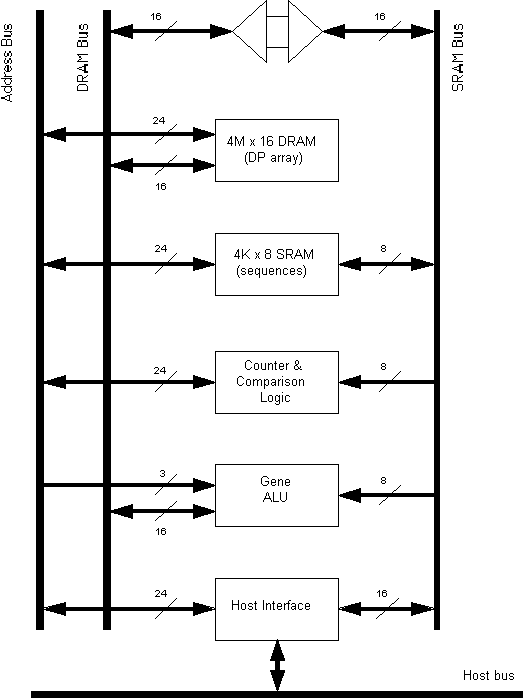
Figure 1:
GSP Block Diagram
Figure 2: Soliton Detector Block Diagram [6]
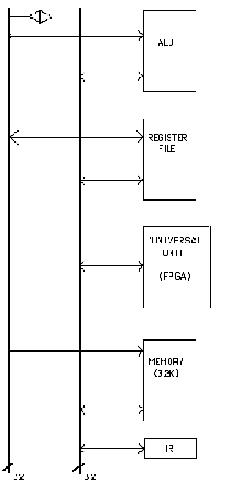
Figure 3: Thayer DLX Datapath
Table 1:
Processor FPGA Usage
FPGA
name function device type
GSP
actelbi4 special-purpose ALU ACT1020-68 (2)
actelcc counter/comparator ACT1020-68
actelsri static ram interface ACT1010-68
actelmx4 10 bit 2-1 mux ACT1010-44
PFT
dagc_contl sign, window, length, router ACT1020-68
master3a master counter ACT1020-68
cntrega counter register bank ACT1020-68
regbank data register bank ACT1020-68
DLX
uuchip universal unit for DLX ACT1020-84
Table 2: FPGA Module Count, Area, and Cost
Device
type logic i/o area
(in2) cost
ACT1010-44
PLCC 295 34 .43 23.25
ACT1010-68
PLCC 295 57 .91 23.25
ACT1020-44
PLCC 546 34 .43 43.30
ACT1020-68
PLCC 546 57 .91 43.30
ACT1020-84
PLCC 546 69 1.32 43.30
Table 3: IC Equivalents for FPGAs
FPGA name count area (in2) pins power (mW) cost
($)
actelbi4 53 10.54 874 12492.5 69.76
actelcc 26 7.03 502 8241 29.80
actelsri 7 1.61 128 2065 7.28
actelmx4 3 .55 48 345 2.64
dagc_contl 41 9.31 644 7882.5 57.97
master3a 33 14.36 624 5878 53.43
cntreg 34 7.88 624 5000 37.92
regbank 42 9.28 780 6560 46.84
uuchip 34 7.52 923 8768 72.27
Table 4: IC/FPGA Ratios
FPGA
name area power pins cost
actelbi4 11.58 65.49 12.85 1.61
actelcc 7.72 19.29 7.38 .69
actelsri 1.77 27.14 1.88 .31
actelmx4 1.29 9.80 1.09 .11
dagc_contl 10.89 15.46 9.47 1.34
master3a 58.71 11.50 9.18 1.23
cntrega 8.66 22.22 9.18 .88
regbank 10.20 24.94 11.47 1.08
uuchip 5.70 24.48 10.99 1.66
Table
5: FPGA Utilization
FPGA name logic/total % logic utilized io/total % i/o utilized
actelbi4 386/546 70.70 44/57 77.19
actelcc 444/546 81.32 55/57 96.49
actelsri 78/295 26.44 51/57 89.47
actelmx4 15/295 5.08 31/34 91.18
dagc_contl 276/546 50.55 56/57 98.24
master3a 501/546 91.76 44/57 77.19
cntrega 490/546 89.74 32/57 56.14
regbank 524/546 95.97 24/57 42.10
uuchip 484/546 88.64 65/69 94.20