Using
Antifuse-Based FPGAs in Performance Critical Digital Designs
Thayer School of Engineering
Dartmouth College
Hanover, NH 03755
barry.fagin@dartmouth.edu
Abstract
We present experimental results
on the use of antifuse-based FPGA's in a performance critical digital design,
performed at the recently completed Thayer Rapid Prototyping Facility. Our case study focuses on the design of a
special purpose ALU for gene sequence analysis.
Our work indicates the existence of highly nonlinear relationships
between design changes and critical path lengths, due to the overwhelming
influence of routing on performance.
This suggests that the standard paradigms for digital design are not
appropriate for FPGA's. We compare our
results to previous work using SRAM-based technology, and discuss the
implications of our results for digital design and rapid prototyping.
1.0
Introduction
We have previously reported in
[1] the results of experimental investigations concerning the use of SRAM-based
FPGA's in high performance digital designs.
This paper describes similar experiments using antifuse-based
devices. Both efforts were performed at
the Thayer Rapid Prototyping Facility [2], now essentially complete.
The
Thayer RPF is an integrated digital systems laboratory, designed to permit all
stages of the design process to be carried out in a single facility. The emphasis is on board-level systems,
consistent with our research objective of producing working hardware
quickly. This is facilitated by the use
of a PCB prototyping system. This system
employs a plotter/etcher and a drill machine.
The plotter/etcher uses commercial inkjet printing technology to spray a
resistive ink on copper film. The film
is then etched with sodium persulfate, dissolving all exposed copper. After a rinse, the ink is scrubbed off with
steel wool, and the film is tin plated.
The drilling machine and laminating equipment are then used to produce a
finished board. Both the plotter/etcher
and the drill are controlled by a PC, using vendor-supplied software.
The
system produces boards that are well behaved electrically, and supports
multilayer prototypes. Minimum trace
width and spacing are both 5/1000 inches.
Figure 1 shows a simple 2-layer, 300 hole board produced at the
RPF. This board took about an hour to
etch and drill.
Figure
1: Sample PCB Prototype Board
2.0 A
Gene Sequence ALU
We are currently using the Thayer
Rapid Prototyping Facility to perform a number of experiments in special
purpose computation. One of these
experiments entails the construction of a special purpose computer for molecular
genetics.
Many
applications of computers in molecular biology are essentially string
comparison problems. A typical
computational task in molecular biology, for example, is the determination of
the relationships between two sequences of DNA. These relationships can be
specified in terms of additions, deletions, and changes of bases. A computerized analysis of these
relationships can aid the molecular biologist in an understanding of both
evolutionary history and biological function.
Algorithms
for solving these problems are well known [3], perhaps more so by computer
scientists than biologists. This type of problem is solved with a dynamic
programming algorithm. The two sequences
to be compared are placed along the top row and left column of a matrix. The value at a particular entry in the matrix
reflects the 'similarity' between the subsequences corresponding to the
appropriate row and column. To determine
the value at a particular cell, the values of the left, north, and northwest
neighbors are examined. The value for
the cell is based on a parametrized weighting of these values, and the process
repeats. As shown in Figure 2, the
computation can proceed in parallel wavefronts along the diagonals of the
matrix.

Figure
2: Gene Sequence Alignment Computation
The
basic operation of this type of computation is a 5-input function, in which the
west, north, and northwest neighbors of cell [m,n] along with nucleotides m and
n in sequences A and B are used to determine the new value of a cell. This suggests that performance can be
improved through the use of a special "gene ALU" that uses a cell's
neighboring values and nucleotide information to calculate a new value, based
on a user-supplied weighting function.
This is shown in Figure 3.
Because the choice of weighting function is itself often an experimental
variable, freezing this function in
hardware is a poor design decision. For this reason, we targeted the gene alu to the Actel
1010/1020 series of FPGAs.

Figure
3: Gene ALU (targeted for Actel
1010/1020 FPGA)
The
basic design for the gene ALU is shown in Figure 4. (The schematic was created using Viewlogic's
Workview® design package, the design entry tool at the Rapid
Prototyping Facility). The three paths
of comparison are easily visible in the design: north values at the top,
northwest in the middle, and west at the bottom. The eight-bit output value appears at the
right of the schematic, going directly to output pads. Figure 4 is hierarchical; boxed symbols
include latches and comparators, also specially designed and associated with
their own schematics.
We
anticipated to improve the performance of the design through a repeated process
of critical path identification, redesign, and resimulation. Our expectation, based on digital design
experience with other technologies, was that each iteration would yield smaller
and smaller delays along the critical path, or perhaps a new critical path on
which the process would be repeated. In
either case, we expected a reasonably linear interaction between designer and
device, in which each iteration would yield performance improvements over the
previous one until a point of diminishing returns was reached. Our actual experience with the design was
quite different.
Figure
4: Gene ALU Schematic
3.0
Timing Analysis
Once
the schematic was created and functionally simulated, we began with the random
pin assignment A of Figure 5. This
produced a critical path of 181.9ns, through the north input path as shown. We then employed the more careful pin
assignment of B in Figure 5, in which all related signals were placed next to
each other. This resulted in a slightly
shorter delay along a different critical path.
We then attempted pin assignment C, and found a new critical path with a
longer delay than the original one.

Figure
5: Pin assignments and critical paths
Further
experimentation yielded similar nonlinear relationships between design changes
and performance. To obtain a clearer
understanding of the phenomenon, we examined the software estimates of the
critical path of 8 points in the design space (2 designs, 2 dies, and 3 pin
assignments). This is shown in Table 1.
Table 1: CRITICAL PATH LENGTHS
pinout
A pinout B pinout C Average
MODIFIED
Average Die
1010 185.8 183.1 218.9 195.9
198.67 Die 1020 186.0 194.6 223.6 201.4
ORIGINAL
Average Die
1010 171.1 169.6 184.5 175.1
188.42 Die 1020 198.2 192.2 214.9 201.8
Average 186.7 187.8 202.6 193.5
We may make several observations
from Table 1. The difference between the
slowest and fastest designs, for example,
is about 31%, a large value considering the similarities between
designs. We see as well that in every
case performance is worse with a larger device.
This is consistent with previous results reported for SRAM-based devices
[1]; the longer net length of designs implemented on larger devices outweighs
their easier routability.
Table
1 seems to describe a chaotic system, one that is extremely sensitive to
initial conditions. Perturbations in
design parameters that would yield small changes in critical path length for other
technologies may yield much larger perturbations for FPGA's. The difference between the original and
modified designs, for example, is a single buffer. Two designs in the same row of Table 1 differ
only by pin assignment, while two designs adjacent to one another in the same
column differ only in the target device.
4.0
Routing and Performance
The key to understanding Table 1
lies in the place and route phase of the design cycle. The routing software may be viewed as a
highly nonlinear function that maps between schematics and FPGA programming
files. This mapping is so irregular that
accurate predictions of performance in response to design changes are
essentially impossible. We note that two points in our design space differing
only in a signal name had a 3% difference in maximum delay and different
critical paths.
Figures
6 and 7 illustrate another aspect of routing and performance. El Gamal et. al. in their description of the
Actel FPGA architecture discuss the uses of both horizontal and vertical
routing tracks for routability [4].
Vertical lines are connected to large numbers of antifuses, which add
parasitic capacitance and slow down signals routed through them. This suggests that designs with many vertical
long lines will show substantially reduced performance, and implies that the
minimization of long lines is an important task of the router. Our examination of different gene alu designs
supports this hypothesis. Figure 6 shows
the number of horizontal lines versus the maximum delay for 34 gene alu
designs, along with a line of best fit.
Since the data points are widely scattered, the equation of the line is
of little interest. Its negative slope,
however, indicates that maximum delay decreases as the number of horizontal
lines increases, as expected.
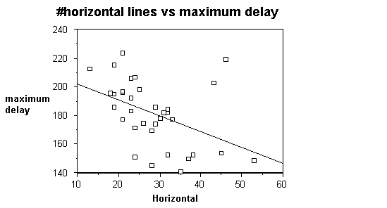
Figure 6
Figure
7 shows a similar plot for vertical lines.
The line of best fit slopes upward, indicating the predicted increase in
delay with the number of vertical lines.
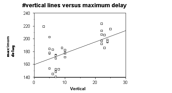
Figure 7
5.0
Conclusions and Practical Observations
Actel FPGAs are now an important part of the Thayer Rapid
Prototyping Facility. We are currently
using hardware and software support for these devices, and are pleased with the
results. Designs place and route
quickly; manual intervention was never
required to achieve a successful route.
However, the relative difference
in sophistication between FPGA devices and FPGA software described in [1] is
further indicated here. The
Actel/Workview interface, for example, does not currently support the simulation
of systems that mix Actel FPGAs with standard TTL parts. Additionally, the Actel architecture is not
transparent; when the timing analyzer describes critical path information, the
designer cannot view the fuse map to see where the problems are. This in turn makes selecting the appropriate
design changes difficult, requiring a heuristic "bag of tricks"
approach to optimize for performance. A
tool that permits the user to see how signals were routed and, if necessary,
edit the fuse map, would not be difficult to write and would assist designers
interested in using antifuse-based FPGAs in performance-critical designs.
Our
experience indicates that the standard mode of interaction between digital
designer and digital design does not apply for FPGAs. The expected linear relationship between
design changes and design performance does not appear, due to the chaotic
interventions of design routing. We
note, however, that while the direction of performance change in response to a
design change may not be known, the magnitude of the change can be bounded by
the fundamental characteristics of the device. Major design changes may thus be
able to move the design into a new region of performance, but fine tuning to
introduce marginal improvements seems impossible. This suggests that the suitability of FPGAs
for a given design depends on performance objectives. For projects in which every nanosecond of
performance is important, FPGA's are not
an appropriate implementation technology. The larger the region of acceptable
performance, the more attractive FPGA's become.
We
note that the conclusions described here are based on a single design. Other projects are currently underway at the
Thayer RPF, including the design of a multiplier for large integers and an
architectural subset of the DLX microprocessor [5]. Future work includes examining the FPGAs
associated with these designs to see if they support the conclusions drawn
here. Additionally, the times
described in this paper are estimated by vendor-supplied software. When the gene alu and other systems are
actually built, these delays should be measured empirically.
Long
term plans at the RPF call for a shift of
focus, using FPGA's in systems for which exacting standards of
performance are less important than the ability to produce a working prototype
quickly. We plan to integrate FPGA's
into board-level systems using the RPF PCB prototyper, concentrating on issues
of trace routing and system testing. We also plan to compare different families of
FPGAs by implementing identical designs with different devices and studying
cost/performance tradeoffs.
6.0
Acknowledgements
The Thayer Rapid Prototyping
Facility has received support from a number of sources, Industrial sponsors include Viewlogic, Actel,
Xilinx, Direct Imaging, and Sun Microsystems.
The gene sequence processor project is supported by a grant from the
Whitaker Foundation, while the completion of the RPF was supported with a grant
from the National Science Foundation, award #CDA-8921062.
7.0
References
[1] Fagin, Barry, "Using
Reprogrammable Gate Arrays in Performance Critical Digital Designs",
Proceedings of the 3rd Microelectronics Systems Education Conference and
Exposition, Santa Clara, CA, 1990, pp 43-60.
[2] Fagin, Barry and Hitchcock,
Charlie, "Rapid Prototyping Without MOSIS: A Minority View",
Proceedings of the 2nd VLSI Education Conference, Santa Clara, 1989, pp 59-67.
[3] Sellers, Peter H., "On
the Theory and Computation of Evolutionary Distances", SIAM Journal of Applied
Mathematics, June 1974, Volume 26, No. 4, pp 787-793.
[4] El Gamal, Abbas et. al.,
"An Architecture for Electrically Configurable Gate Arrays", IEEE
Journal of Solid State Circuits, Vol. 24, No. 2, April 1989.
[5] Patterson, David and
Hennessy, John, Computer Architecture: A Quantitative Approach, Morgan Kaufmann
Publishers Inc., San Mateo, CA, 1990.