Abstract
We
describe our prototyping of a
functioning DLX microprocessor, based on the 32-bit instruction set
architecture developed by Patterson and Hennessy. This architecture is an emerging academic
standard, but to our knowledge has yet
to be successfully prototyped. Our
implementation of DLX is a 12" x 15" 2-layer circuit board,
containing 59 chips and running on a 2 MHz clock. Our machine was developed at the Thayer Rapid
Prototyping Facility, a laboratory for the rapid construction and evaluation of
digital systems.
1.0 Introduction
The DLX
microprocessor is a 32-bit RISC CPU,
designed by David Patterson and John Hennessy and described in detail in
[1]. This description includes instruction set formats, opcode mnemonics, and a
basic datapath. A compiler and simulator
are also available, greatly simplifying the task of developing a complete
working system. Despite this, while DLX
has been simulated extensively at many different sites (see for example [2] and
[3]), it has to our knowledge never been implemented.
This paper
describes our implementation of the DLX microprocessor. The resulting system was produced entirely on
site, and correctly executes C programs compiled with the DLX compiler. We have learned a great deal from building a
working system, and here share our insights for others interested in
implementing DLX and other complex microsystems.
We begin
with an overview of the Thayer Rapid Prototyping Facility, our laboratory for
the rapid production of digital systems.
We then briefly discuss the DLX architecture, and describe our
implementation in considerable detail.
We discuss how Thayer DLX programs are executed, identify the
significant problems we encountered, and discuss how they were solved. Conclusions are presented, along with directions
for future work.
2.0 The Thayer Rapid Prototyping Facility
Approximately
three years ago, we began a concerted research effort into providing an
enhanced rapid prototyping capability for our research in digital system
design. We had identified several
problems with VLSI-based prototyping approaches [4], particularly for sites
where local fabrication was not possible, and decided to adopt a PCB-based
approach. We envisioned a facility where
users could walk in with an idea and walk out with hardware, all without ever
having to leave the lab. The result was
the Thayer Rapid Prototyping Facility.
The Thayer
RPF is designed to provide hardware and software assistance for each step of
the design process. Our view of this
process is shown in Figure 1. The design
begins with functional specification and a high-level block diagram. Hardware components are selected, and the
design entered with schematic capture tools.
The design is simulated , and a netlist generated. After placement, the design is then used as
input to a PCB layout program. Layout
and routing tools produce a board description file, which is turned into a
board using a PCB prototyper. The resulting board is populated with ICs and
tested.
The goals of
the Thayer RPF are 1) to have all steps of this process performed in the same
laboratory, and 2) to produce working prototypes as quickly as possible. To achieve these goals, we have constructed
an integrated environment of commercial products. We have chosen the Sun Sparcstation as the
main workstation for the Thayer RPF.
Currently, we have four color workstations in the laboratory. The Workview® tool package, from
Viewlogic Incorporated, is used to accelerate the schematic capture and
simulation stages of the design process.
Workview provides a complete schematic capture and simulation package,
including back-annotation, hierarchical schematics, an extensive parts library,
and support for device modeling. We also
have an extensive array of field programmable gate array support, including
Actel, Altera, and Xilinx development systems.
For PCB
layout, we are using the Racal-Redac PCB system, running on an IBM PC. We have written our own software in house
that assists in the translation of Workview netlists to the format Racal-Redac
requires.
The RPF is
perhaps unique as an academic laboratory in that it has the capability of
producing printed circuit boards on site, in the same room in which systems are
designed. The RPF employs a PCB
prototyping system developed by Direct Imaging Incorporated, in which a
resistive ink is sprayed on copper sheets and then etched with sodium
persulfate. The ink is then scrubbed off,
the sheets tin plated and automatically drilled, and then assembled into a
finished prototype.
System
testing is the final stage of the design process. This requires a sophisticated pattern
generator and logic analyzer, one that interfaces easily with the simulation
tools of the CAD system being used and permits
rapid comparison of simulation output vectors with observed output
vectors. The Thayer RPF uses the HP
16500A logic analyzer for system bringup and test. This device has proven extremely effective in
the final stages of the system prototyping process.
The Thayer
Rapid Prototyping Facility has been involved in several successful experiments
in rapid digital system design. In
addition to the DLX microprocessor, other projects include the design of a
computer for gene sequence analysis, an FHT transform engine, and a real-time
data processor for rocket telemetry. For
further information on these and other projects, the reader is referred to [5],
[6], [7], and [8].
The problems
of producing working systems in a university environment are well known [9].
These problems include continuity of personnel, publication pressures,
and resource availability. We have
experienced all these difficulties in our efforts to develop a rapid
prototyping laboratory. Nonetheless, our
experience with the RPF confirms the positive experience of other researchers
in this area; rapid prototyping capabilities make valuable contributions to
both teaching and research that simulation cannot. Our prototyping of the DLX microprocessor is
a case in point.
3.0 DLX
Architecture
For readers
unfamiliar with the DLX architecture, we give a brief overview of it here. Other readers may skip to the next
section. For a more detailed
presentation, the reader is referred to [1].
DLX is a
32-bit microprocessor architecture, with 32 general purpose registers and a
hard-wired zero in R0. Memory is Big
Endian byte addressable (i.e. byte 0 is in the most significant position of the
word), and all instruction accesses are aligned.
The DLX
integer instruction set is shown in Table 1.
(A floating point extension of the architecture is also described in
[1], which we did not implement). There
are three basic classes of instruction: data transfer, arithmetic/logical, and
control flow. Instruction formats are
shown in Figure 2. We note that the DLX instruction set is highly
streamlined. The number of instructions
and instruction formats is small, and instruction decoding is simple.
One
suggested DLX datapath is shown in Figure 3.
Consistent with the instruction set, the datapath has two source busses
and a destination bus. A 32-bit ALU is
responsible for basic arithmetic and logical functions, with interaction to
memory handled by a Memory Address Register and a Memory Data Register. Interrupt addresses are stored in the
Interrupt Address Register, while instructions are fetched with a PC. We see from the datapath that most
instructions can execute in one cycle.
In general,
we note that the DLX microprocessor has a streamlined instruction set, with a
few simple instruction formats and operations that are easy to decode. The architecture is carefully described, and
comes with a publicly available C compiler and simulator. All these features make it an ideal candidate
for microsystem prototyping.
4.0
Implementation
Our
implementation of DLX is a 2-layer 12" x 15" printed circuit board,
shown in Figure 4. This board was
manufactured in the RPF with the PCB prototyper discussed earlier. The board contains 59 chips and consumes 12.5
watts of power.
A block
diagram of the Thayer DLX datapath is shown in Figure 5. Comparing with Figure 3, we see that the
principle differences are 1) the adoption of a 2-bus architecture, and 2) the use of a so-called "universal
unit", or UU.
We chose a
2-bus architecture for three reasons: 1) to match our available register files, which shared input
and output pins, 2) to improve the routability of the board, and 3) to simplify
the machine. This decision reflects a
consistent willingness to sacrifice performance for an increased probability of
producing a working prototype under time constraints. We expect that others
interested in prototyping DLX will face similar tradeoffs.
The UU is a
field programmable gate array, initially adopted to implement a 32-bit barrel
shifter. As the design progressed,
however, we discovered that more and more logic could be added to it without increasing chip count or power
consumption. Thus the shifter became the
UU, containing both the (nontrivial) sign-extension logic required by the DLX
instruction set and the memory alignment circuitry. The ability to incorporate new logic into our
design quickly and easily was crucial to its success; the use of a field
programmable gate array was absolutely essential.
4.1 Program Execution
The Thayer
DLX communicates with a Macintosh computer using a UART; binary files are
downloaded over an RS-232 link into 32K of on-board SRAM and then executed.
To run
programs on the Thayer DLX, the processor board must first be powered up and
reset. A boot ROM initializes the
register file, interrupt vectors and the UART, and then waits for incoming
files over the RS-232 link.
To execute
programs, the user begins by creating a C program and compiling it with the
public domain DLX compiler (dlxcc). This
produces an ASCII file of DLX instructions.
The first few lines of a compiler output file are shown in Figure 6.
The DLX
instruction file is then assembled using a modified version of the DLX simulator
(dlxsim), producing an ASCII hex file of addresses and data. A portion of this file is shown in Figure
7. This file is then downloaded to the
DLX board over the serial line; the boot ROM program reads the incoming
characters and stores them in SRAM. Only
the first two fields of each line are processed. When an address of 0xFFFFFFFF is read, the
board stops the download and begins executing the program.
In addition
to board initialization code, the DLX boot ROM contains UNIX library
functions. Current system calls include
printf, putc, and getc, which perform simple output on the Macintosh. We use memory-mapped I/O, allocating a
certain portion of the address space to the UART. Other functions include integer
multiplication and division, which are performed in software. All functions and library routines are
written with DLX instructions. Our
experience indicates that having students write ROM code for library functions
teaches them lessons about hardware/software tradeoffs more effectively than
any classroom exercise.
4.2 Errors Found
A computer
system must be considered as a complete whole; the compiler, assembler,
instruction set, hardware, and other components interact in subtle ways. The implementation and bringup of DLX require
the ability to find and correct bugs virtually anywhere. As expected, the majority of errors occurred
at subsystem interfaces; subsystem components, on the whole, worked
correctly. Typical examples of this were
1) human errors in the conversion of the DLX schematic netlist to the PCB
netlist, resulting in unrouted traces, and 2) an inability for certain
instructions to access the UU properly, due to a simulation error at the
interface between the FPGA and TTL parts of the design. Human error was, of course, also a
factor. 17 connections had to be
wire-wrapped manually; some of these were later found to be incorrect. Even the more mundane problems did not escape
us; we had chips inserted incorrectly, poor solder connections, and improperly
wired components due to misread documentation.
Of greater
significance were errors identified in the DLX software and documentation in
the course of debugging our board. We
obtained our software via anonymous ftp in November, 1990, and based our
implementation of DLX on the 1990 edition of [1]. The distribution includes source code and
examples.
It is
remarkable that we found as few errors as we did, since to our knowledge DLX
has never been completely implemented.
Nonetheless, since these problems will be of interest to others working
with DLX, we mention them below:
1) Unsigned set
instructions. In addition to SETxx instructions, which set
the condition code based on a signed comparison, the compiler generates
unsigned SETxxU instructions. We
discovered this only after our board was designed, and were surprised to find
them as they were not mentioned in the documentation. We redesigned the DLX finite state machine to
support these instructions without much effort, and in the process discovered a
design error in the setting of the overflow condition code.
2) Compiler errors in shift expressions. Our version of the DLX compiler would not compile C shift
expressions of the form "a << b", with a and b variables. We corrected this problem by modifying the
machine description file.
3) Compiler errors in logical negation. The compiler would
accept logical negation operations (e.g.
~a), but the resulting code would not be accepted by the simulator. Changing the machine description file also
fixed this problem.
4) Formats of SLLI, SRLI, and
SRAI instructions. The SLLI, SRLI, and SRAI
instructions were encoded by the assembler as R-format instructions. We believed this to be incorrect, and recoded
them as I-format instructions.
5) Address calculations of labels. Forward references in the assembler were not handled
properly, resulting in incorrect address values for labels in assembly files.
Other
modifications were made to the software to suit our particular implementation
of DLX. We cannot overemphasize the
importance of source code access to our implementation efforts.
5.0 Performance
Our
prototype is a slow machine, running at 2MHz.
This is slower than any of the academically-developed prototypes
described in [9]. We believe this to be
due to 2 factors: 1) our willingness to choose less aggressive technology and
trade off performance for increased probability of the production of a
functioning prototype, and 2) the fact
that DLX is the first major project completed at the RPF. We note that a later RPF project, the Gene
Sequence Processor, runs at 10 MHz [8], although readers should use caution in
comparing the two devices.
Additionally, DLX CPI figures are high for a streamlined
instruction set. Of the 66 instructions
we implemented, 32 require 5 cycles, 23 require 6, and 11 require 7, giving a static
average CPI of 5.7. Many well-known
techniques could be employed to reduced CPI, including pipelining, prefetching,
and delayed memory accesses. Similarly,
using different IC's (in particular, eliminating the FPGA) could yield a
significantly faster clock.
These
figures represent a tradeoff between two design goals: making the system fast
versus making the system quickly.
Virtually all our design decisions, the 2-bus architecture, the use of
an FPGA, the simple control strategy, and others, reflect a willingness to
tradeoff performance for a working system.
It seems
clear that if building working hardware means consistently losing performance,
then much of the motivation for building hardware is lost. We believe, however,
that technology advances the functionality/performance curve, just as it
advances cost/performance. (For example,
as FPGA technology progresses, more
functionality can be included in designs with faster clocks). As the technology for rapid prototyping
improves, and as our familiarity with DLX increases, we anticipate building
faster and faster versions of both DLX and other digital systems in less and
less time. Plans for the next iteration
of DLX include pipelining and floating point processing.
6.0 Conclusions
With a few
notable exceptions (see for example [10]), universities have been difficult
places to build functioning hardware.
The translation of ideas from simulations to working prototypes is
believed to be unnecessary and/or
insurmountably difficult.
Our work
suggests that advances in rapid prototyping technology force a reevaluation of
this position. The emergence of open
architectures, field programmable gate arrays, and PCB prototypers suggest that
working hardware can be developed where previously simulation was all that
could be expected. This means that
students learn more; they find the design experience more rewarding when they
build something that works.
But in
addition to pedagogical benefits, rapid prototyping has significant scientific
advantages. Results obtained from
working hardware are inherently more credible than those from simulation; simulation results are virtually impossible
to reproduce reliably, while hardware results are much more likely to be
confirmed elsewhere. Constructing
hardware is in a very real sense an experiment that tests a hypothesis,
permitting strong inferential techniques and reproducibility of results to be
employed in a manner closer to that of the physical sciences.
We have
offered evidence in support of these conclusions in this paper, discussing the
development of a functioning DLX microprocessor in an academic laboratory. This effort makes extensive use of rapid
prototyping technology, embodied in an on-site laboratory for digital system
construction. The resulting project has
benefited both our teaching and research efforts; we have learned a great deal
about microsystem prototyping and the use of field programmable gate
arrays.
Future work
will include faster pipelined versions of DLX, the addition of floating point
capability, and the prototyping of more advanced digital systems. We are currently prototyping a pipelined
version of DLX, using a multilayer PCB design, and expect implementation
results shortly. We hope others will
join us in our efforts to move universities away from simulation and towards
the increased production of working hardware.
We believe the rewards will prove worth the effort.
7.0 Acknowledgements
The authors gratefully
acknowledge the contributions of Professor Charles Hitchcock, Todd Thayer and
Evan Gewirtz in bringing up Thayer DLX.
The Thayer Rapid Prototyping Facility is supported by a variety of
sources, including the Whitaker Foundation, Actel, Altera, Xilinx, Sun
Microsystems, Viewlogic, National Semiconductor, and Direct Imaging Incorporated. Additional support was provided by the
National Science Foundation, award #CDA-8921062.
8.0
References
[1] Patterson, David and
Hennessy, John "Computer Architecture: A Quantitative Approach",
Morgan Kaufmann Publishers Inc., San Mateo, CA,
1990.
[2] Reese, Bob and Harden,
Jim "Efficient Use of a Behavioral
Simulator in an Introductory Computer Architecture Course", Proceedings of
the 4th Microelectronics System Education Conference and Exposition, San Jose,
CA, 1991, pp 107-116.
[3] Siewiorek, Daniel et. al., "The Use of
Verilog in an Introductory Computer Architecture Course", Proceedings of
the 3rd Microelectronics System Education Conference and Exposition, San Jose,
CA 1991, pp 139-148.
[4] Fagin, Barry and Hitchcock,
Charles, "Rapid Prototyping Without MOSIS: A Minority View",
Proceedings of the 2nd Annual VLSI Education Conference, San Jose, CA, 1991, pp
59-67.
[5] Erickson, Adam and Fagin,
Barry "Calculating the FHT in Hardware", IEEE Transactions on Signal Processing, June 1992, pp 1341-1353.
[6] Fagin, Barry "The
Effects of Field Pro- grammable Gate Arrays on the Digital System Design
Process", Technical Report, Thayer School of Engineering, Dartmouth
College, Hanover NH 03755.
[7] Fagin, Barry "Using Antifuse-Based FPGAs in
Performance-Critical Digital Designs",
Proceedings of the 4th Microelectronic Systems Education Conference and
Exposition, San Jose, CA, 1991.
[8] Fagin, Barry "FPGA
Utility in Special and General Purpose Processors", special issue of the Journal of VLSI Signal Processing on
Field Programmable Gate Arrays, to appear.
[9] Dollas, Apostolos and Chi, Vernon,
"Rapid System Prototyping in Academic Laboratories of the 1990's",
Proceedings of the 1st International Workshop on Rapid System Prototyping,
Research Triangle Park, North Carolina, 1990, pp 38-45.
[10] Poulton, John "Building Microelectronic Systems in a
University Environment", Proceedings of Advanced Research in VLSI 1991,
Santa Cruz, CA, pp 387-400.
9.0 Figures and Tables
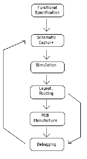
Figure 1: Digital System Design
at the Thayer RPF

Figure 2: DLX Instruction
Formats
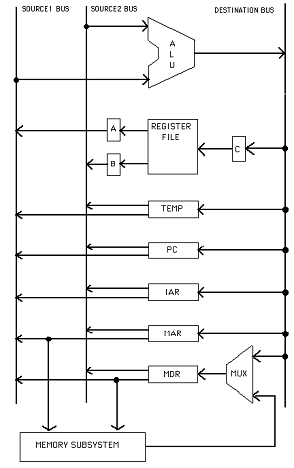
Figure 3: Integer DLX Datapath
[1]
Figure 4: Thayer DLX Board
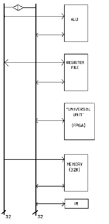
Figure 5: Thayer DLX Datapath
.text
.align 2
.global _fib
_fib:
;; Save the old frame pointer
sw -4(r14),r30
;; Save the return address
sw -8(r14),r31
;; Establish new frame pointer
add r30,r0,r14
;; Adjust Stack Pointer
add r14,r14,#-16
;; Save Registers
sw 0(r14),r3
sw 4(r14),r4
lw r4,0(r30)
addi r3,r0,#2
sgt r1,r4,r3
bnez r1,L2
...
Figure 6: Compiler output
00000000
0bff7ffc j 0xffff8000 ; trap #0 (warm start)
00000004
0bff7ffc j 0xffff8004 ; trap #4 (mult and div)
00000008
0bff7ffc j 0xffff8008 ; trap #8 (UART putc)
0000000C
0bff7ffc j 0xffff800c ; trap #12 (UART getc)
00000010
0bff7ffc j 0xffff8010 ; trap #16 putch( char c)
00000014
0bff7ffc j 0xffff8014 ; trap #20 getch( char c)
00000018
0bff7ffc j 0xffff8018 ; trap #24 getcc( char c)
; (no wait getch)
0000001C
0bff7ffc j 0xffff801c ; trap #28 printf
00000020
0bff7ffc j 0xffff8020 ; trap #32 sprintf
00000024
0bff7ffc j 0xffff8024 ; trap #36 gets
00000100
24000000 trap #0 ; This trap has no
return
00000104
24000008 trap #8
00000108
2be00000 jr r31
0000010C
2400000c trap #12
...
Figure 7: Assembler output
Table 1: DLX Instructions [1]
LB,LBU,SB load
byte, load byte unsigned, store byte
LH,LHU,SH for
halfword
LW,SW for
word
MOVI2S,MOVS2I special
purpose register access
ADD,ADDI,ADDU,ADDUI signed and unsigned add, add immediate
SUB,SUBI,SUBU,SUBUI for subtraction
MULT,MULTU,DIV,DIVU signed and unsigned 32-bit multiply
AND,ANDI logical
AND, AND immediate
OR,ORI for
OR
XOR,XORI for
XOR
LHI load
high immediate; loads upper half of register
SLL,SLLI shift
left logical, immediate
SRL,SRLI shift
right logical, immediate
SRA,SRAI shift
right arithmetic, immediate
Sxx,SxxI conditional,
conditional immediate
xx indicates test: LT,GT,LE,GE,EQ,NE
BEQZ,BNEZ Branch
if register equal/not equal to zero
J,JR jump
(PC offset), jump (register target)
JAL,JALR jump
and link, PC relative or register target
TRAP OS call
RFE return
from exception