Dartmips: A Case Study In Quantitative Analysis Of Processor Design Tradeoffs Using FPGAS
Barry Fagin and John Erickson
Thayer School of Engineering
Dartmouth College
Hanover, NH 03755 USA
Abstract
The high integration and sophisticated CAD tools associated with FPGAs permit an increase in both the complexity of systems that can be analyzed in an engineering laboratory and the precision with which the analysis can be performed. This paper presents an experimental analysis of one such system: DartMIPS, an implementation of the MIPS R3000 architecture using FPGAs. We present qualitative and quantitative analysis of four incrementally modified designs, from a sequential implementation to a fully pipelined design with data forwarding. We report as well our insights in implementing complex systems using FPGAs, and discuss directions for future work.
INTRODUCTION
Designers face a variety of tradeoffs when implementing a system. The problem space is too large to search exhaustively, while implementations are typically completed under severe time constraints. This means that detailed quantitative analyses of design alternatives are almost never performed: the effort is too time-consuming and costly.
FPGAs, however, may make this process easier. The existence of well-defined relationships between logic in a design and the area resources required by that logic can permit more detailed analysis of design tradeoffs. As FPGAs become denser, researchers may find themselves in the enviable position of being able to construct systems of increasing complexity while simultaneously being able to analyze them in increasing detail.
To test out these ideas, we are currently experimenting with a number of complex digital systems using FPGAs at the Thayer Rapid Prototyping Facility, a laboratory for the rapid construction and evaluation of digital systems. One such system, an implementation of the MIPS processor architecture, is described here. We chose the MIPS design because, as a RISC microprocessor, it combines non-trivial functionality with a well-defined specification and an extensive history of previous quantitative analysis. For a previous study that measured the effectiveness of FPGAs in both special and general purpose processors, the reader is referred to (Fagin 1993).
PROJECT OVERVIEW
A pipelined implementation of a subset of the MIPS R3000 instruction set architecture as described by Kane (1992) was successfully designed and verified, through functional simulation, using Actel's family of FPGAs (1992) as the target technology. The processor uses a classic five-stage datapath pipeline; a split instruction/data memory model was chosen to simplify design work.
Four distinctive DartMIPS processors were considered, each promising higher performance along with increased logical complexity. Our process of gradually implementing the pipelined processor follows a typical textbook development of pipelining as described by Patterson and Hennessy (1990, 1993), and permitted us to identify the area cost of various pipeline features. This section introduces the designs referred to elsewhere in this paper.
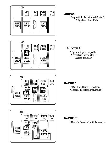
a. DartMIPS1: a sequential, FPGA-based implementation of the R3000 ISA. Although this design is not pipelined, it does contain a pipelined datapath with distributed control logic. Only one instruction is allowed to propagate down the pipeline at a time. This approach consumed more logic than a purely sequential design effort might, but greatly facilitated the creation of succeeding designs.
b. DartMIPS2.0: A simple pipelined implementation, providing no hardware interlocking. This version provided pipelined execution with minimal changes to our sequential design. It assumes a compiler capable of hazard detection and avoidance; all data dependencies must be resolved in software.
c. DartMIPS2.1: A pipelined implementation with data hazard detection. Detected hazards are resolved by injecting stalls into the pipeline and refetching until the hazard producing condition clears.
d. DartMIPS2.2: The final pipelined implementation with data hazard detection, this time resolving potential hazards with the use of forwarding logic, or by stall injection in the case of register reads after memory loads.
Actel FPGAs were the target technology for all functions of the DartMIPS family of processors except for the 2x32x32 Register File, which was implemented with a Xilinx 4005 (1992) device, and the Instruction and Data Memories, where standard SRAMs were used. We felt that the abundance of on-chip fast RAM made the Xilinx parts better suited than the Actel for implementing the 2x32x32 (2k) bits of storage that the Register File requires. While just one Xilinx XC4005 was required, we would need four Actel A1280s to achieve the same fast, uniform storage.
Figure 1 presents an overview of the relationship between the different DartMIPS implementations:
Figure 1 Evolution of the DartMIPS Processor
c.
The DartMIPS Subset of the MIPS ISA
For completeness, our subset of the MIPS ISA is reviewed here. The MIPS R2000/R3000 processor architecture is a 32-bit design with single-word instructions. Immediate (I-Type), Jump(J-Type), Register(R-Type) addressing modes are supported. The architecture calls for 32 general-purpose registers, with R0 hardwired to zero. Instructions must be located in memory on word boundaries, but data may be byte-addressed with proper alignment based on the specific instruction. The MIPS R2000/R3000 architecture also calls for an on-chip System Control Processor which is responsible for memory management including the Translation Lookaside Buffer, and contains the Exception and Control registers.
All variations of DartMIPS implement a subset of this architecture. We did not implement coprocessor functionality, nor did we include a Multiplier/Divider. Both of these units would have added additional design and verification complexity significantly beyond the goals of this project. We did, however, include a small amount of logic to support the detection and handling of overflow and misaligned address exceptions, as well as instructions to provide access to these resources.
The DartMIPS CPU Instruction Set is listed in Table 1:
Table 1
DartMIPS Instruction Set
|
LB, LBU, SB |
Load Byte, load byte unsigned, store byte |
|
LH, LHU, SH |
...for Halfword |
|
LW, SW |
...for Word |
|
LWL, SWL |
Load Word left, Store Word left |
|
LWR, SWR |
Load Word right, Store Word right |
|
ADD, ADDU, ADDI, ADDIU |
Add signed/unsigned, R-/I-Type |
|
SUB, SUBU |
Subtract, signed/unsigned |
|
SLT,SLTU, SLTI, SLTIU |
Set less than, signed/unsigned, R-/I-Type |
|
AND, ANDI |
Logical AND, AND immediate |
|
OR, ORI |
Logical OR, OR immediate |
|
XOR, XORI |
Logical XOR, XOR immediate |
|
NOR |
Logical NOR |
|
LUI |
Load Upper Immediate |
|
SLL, SLLV |
Shift Left Logical, variable |
|
SRL, SRLV |
Shift Right logical, variable |
|
SRA, SRAV |
Shift Right Arithmetic, variable |
|
J, JAL |
Jump, Jump & Link |
|
JR, JALR |
Jump to Register, Jump & Link to Register |
|
BEQ, BNE |
Branch on Equal, not equal |
|
BLEZ, BGTZ |
Branch on Less Than Or Equal to Zero, greater than zero |
|
BGEZ |
Branch on Greater Than Or Equal to Zero |
|
BLTZAL |
Branch on Less Than Zero & Link |
|
BGEZAL |
Branch on Greater Than Or Equal to Zero and Link |
QUALITATIVE DISCUSSION OF DARTMIPS IMPLEMENTATIONS
We now consider qualitatively the design changes that were made as we progressed from the sequential DartMIPS1 to DartMIPS2.2, the final pipelined implementation. First the structure of the sequential design will be reviewed; then each new, pipelined machine will be presented with an emphasis on new functionality and associated new logic.
Sequential Execution: DartMIPS1
The goals of this multicycle implementation were two-fold: to provide an Actel-based emulation of the MIPS architecture, and to provide a starting point for a more complex, fully-pipelined implementation. We therefore tried to anticipate as much of the final pipelined design as possible, which meant creating a multicycle design that was logically more complex than necessary (Erickson 1993). We discovered, however, that the logical organization we adopted lent itself nicely to verification and iteration, simplifying our analysis greatly. In the end, we found that it was easily pipelined, saving us much design effort.
The sequential DartMIPS has a pipelined data path and sequential control. The data path was broken into five blocks, corresponding with the five stages of instruction execution in a pipelined processor:
(1) if: Instruction Fetch
(2) id: Instruction decode & register fetch
(3) ex: Execute & Address calculation
(4) mem: Memory Access
(5) wb: Register write-back
Figure 2 presents a block diagram of the DartMIPS1 design:
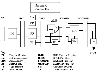
Figure 2 Sequential DartMIPS Block Diagram
Our pipelined data path is very typical of simple pipelined RISC processors, the difference being that in our sequential machine only one instruction will be in the pipeline at a time. A separate control block was created for each pipeline stage, with most inputs for each control block coming from the appropriate stage. The machine was made "sequential" by supplying one common opcode to all control blocks. The phase of execution for the single instruction propagating down the pipe was controlled by a five-bit parallel output shift register, each output corresponding to a phase and enabling the appropriate control logic.
Pipelining: DartMIPS2.0
Opcode pipelining. The first step in converting to pipelined control was to pipeline the opcode in parallel with the data, thus allowing multiple instructions to be present in the pipeline at any instant. This required an additional six bits to be added to the pipeline registers following the ID, EX, and MEM stages.
Link hazard detect. Originally it was not our intention to provide hazard detection in the DartMIPS2.0 design, but when link-related hazards arose during the verification of DartMIPS2.0 we chose to implement the necessary interlocking in that design as well as the final versions. Link hazards occur when a link-type instruction (JAL, JALR, BLTZAL, & BGEZAL) are in the ID stage while the instruction in the WB stage wants to write to the register file. Since both instructions need write access to the register file, a resource conflict occurs. Our solution was to propagate a nop and refetch the instruction; this continues until the hazard clears. Strictly speaking, the logic associated with these changes was NOT required to make pipelining work.
Other changes. Minor changes were made to each of the control blocks to achieve proper pipeline functionality, plus a small amount of 'glue' logic was added at the top level. Typically the problems we encountered were subtle: control blocks would decode properly in the context of sequential execution, but would cause strange errors when piped. All of these control logic problems were easily fixed by rewriting the PALASM equations describing the outputs.
Pipelining with Hazard Detection: DartMIPS2.1
This version of the pipelined design improves on DartMIPS2.0 by providing data hazard detection . Hazards are resolved by propagating a nop instruction down the pipeline, holding the offending instruction in place until the hazard clears, and refetching the following instruction. We deal with Execution and Memory hazards, along with the Link hazard previously described. DartMIPS does not have Writeback hazards, since the processor can performs a register file write and read within one processor cycle.
Execution hazards. EX hazards occur if the instruction currently reading the register file in the ID phase is reading the same register that will soon be written to by the instruction in the EX phase. This hazard is detected by comparing the destination register specifier in EX with the read register specifier in ID, while monitoring the respective opcodes to ensure that such a hazard really would have arisen. About half of the logic in the EX_HAZARD block is dedicated to detecting Execution hazards.
Memory hazards. MEM hazards occur if the instruction currently reading the register file in the ID phase is reading the same register that will soon be written to by the instruction in the MEM phase due to a LOAD instruction. This hazard is detected by comparing the destination register specifier in MEM with the read register specifier in ID, while monitoring the respective opcodes to ensure that such a hazard really would have arisen. The other half of the logic in the EX_HAZARD block is dedicated to detecting memory hazards.
Resolving hazards with stalls. In this version of DartMIPS hazards are resolved by injecting nop cycles, equivalent to stalling the pipeline. Execution, Memory, and Link hazards are detected in the ID phase of the pipeline. Values currently held in the IF/ID pipeline register must be preserved (i.e. not updated at the next system clock); this is accomplished simply by disabling the pipeline register at the next clock. Finally, the instruction just fetched must be re-fetched from the instruction memory; this is accomplished by preventing the PC from being updated with a new value.
Pipelining with Data Forwarding: DartMIPS2.2
The final version of DartMIPS included logic to resolve most data hazards by data forwarding, rather than by injecting stall cycles. By forwarding the outputs of either the ALU or the MEM pipeline registers back to the input MUXes of the ALU we can eliminate Execution hazards; forwarding the output of the MEM pipeline register back to the ALU input MUXes also eliminates Memory hazards. The end result of forwarding is an increase in CPU performance, since we are now able to use data as soon as it becomes available rather than waiting for valid data to propagate through the pipeline and the register file.
Forwarding control. The purpose of the forwarding control logic in the EX phase is to detect the conditions under which forwarding must occur and assert the proper control values to the ALU input MUXes to cause the appropriate result to be forwarded. This logic is similar in complexity to the hazard detect logic of the previous version, consisting mainly of register-select-code-wide comparators, but must reside in the EX phase during which the forwarding actually takes place.
Forwarding muxes. Forwarding provides two additional new input choices for the ALU. Previously the 'B' input had a 32-bit-wide, 2:1 MUX; this grows to 4:1, but does not increase the logic module complexity since 2:1 and 4:1 MUXes have the same LM count. The previously unMUXed 'A' input now requires a 32-wide 4:1 MUX to be added, increasing the LM count.
RAL hazard resolution. Unfortunately, data forwarding does not eliminate all potential data hazards. A read after load (RAL) hazard occurs if a register is used immediately after a load to that register, implying that the operand would just be coming in from the Data Memory when it is required in the EX stage. Forwarding is not acceptable here, since the EX stage needs valid operands early but memory data is not guaranteed valid until the end of the cycle. The instruction with the read must be delayed one pipeline cycle, allowing the valid memory data to propagate through the EX/MEM pipelined register, where it may then be forwarded to the EX stage. This was implemented with a simple detection circuit and combined with the link hazard logic in the ID stage.
QUANTITATIVE DISCUSSION OF DARTMIPS IMPLEMENTATIONS
We now consider the quantitative impact of the design changes that were made as DartMIPS evolved from sequential to pipelined. We note that the numbers presented here are taken prior to placement and routing, and could change due to logic optimization if the design process is carried further. The data for the Sequential DartMIPS implementation will be presented as a baseline, followed by the incremental growth due to the design evolution.
.Logic Module Utilization
Table 2 provides a summary of the logic module utilization of the unpartitioned, sequential DartMIPS design, also presented in (Erickson 1993):
Table 2 Logic Module Utilization, Sequential DartMIPS
|
Pipeline Stage |
Control |
Datapath |
Pipeline |
Total/Stage |
|
IF |
246 |
0 |
56 |
302 |
|
ID |
773 |
36 |
169 |
978 |
|
EX |
35 |
924 |
197 |
1156 |
|
MEM |
36 |
40 |
128 |
204 |
|
WB |
39 |
112 |
129 |
280 |
|
TOTALS |
1129 |
1112 |
679 |
2920 |
Our simple pipelined design introduced the following changes:
(a) Opcode forwarding: 76 LMs
(b) Other logic: 82 LMs
Thus the total impact was an increase of 158 LMs, or about 5%. The new logic module utilization is summarized in Table 3:
Table 3 Logic Module Utilization, DartMIPS2.0
|
Pipeline Stage |
Control |
Datapath |
Pipeline |
Total/Stage |
|
IF |
247 |
0 |
56 |
303 |
|
ID |
798 |
36 |
189 |
1023 |
|
EX |
19 |
932 |
248 |
1199 |
|
MEM |
39 |
40 |
157 |
236 |
|
WB |
47 |
112 |
158 |
317 |
|
TOTALS |
1150 |
1120 |
808 |
3078 |
DartMIPS2.1 introduced the following changes:
(a) Execution hazard detection: 54 LMs
(b) Memory hazard detection: 26 LMs
(c) Related Glue logic: 13 LMs
(d) Link Hazard Detect & resolve: 28 LMs
Thus the total impact was an increase of 121 LMs over DartMIPS2.0, or about 4%. The new logic module utilization is summarized in Table 4:
Table 4 Logic Module Utilization, DartMIPS 2.1
|
Pipeline Stage |
Control |
Datapath |
Pipeline |
Total/Stage |
|
IF |
247 |
0 |
56 |
303 |
|
ID |
828 |
36 |
189 |
1053 |
|
EX |
78 |
932 |
248 |
1258 |
|
MEM |
71 |
40 |
157 |
268 |
|
WB |
47 |
112 |
158 |
317 |
|
TOTALS |
1271 |
1120 |
808 |
3199 |
Finally, the pipelined version of DartMIPS with data forwarding, DartMIPS2.2, shows an increase in control logic complexity over the stalled version, but with new MUXes added at the 'A' input of the ALU in the EX stage and RAL hazard detection in the ID stage. Table 5 shows the resulting logic module complexity. Figure 3 provides a comparison of the logic module complexity of the four implementations, by pipeline stage.
Table 5 Logic Module Complexity, DartMIPS 2.2
|
Pipeline Stage |
Control |
Datapath |
Pipeline |
Total/Stage |
|
IF |
247 |
0 |
64 |
311 |
|
ID |
878 |
36 |
189 |
1103 |
|
EX |
93 |
978 |
248 |
1319 |
|
MEM |
39 |
40 |
157 |
236 |
|
WB |
45 |
111 |
158 |
314 |
|
TOTALS |
1302 |
1165 |
816 |
3283 |
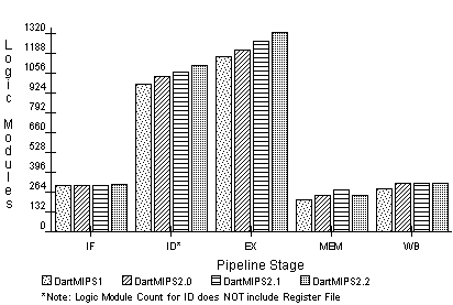
Figure 3
Logic Module Usage Per Pipeline Stage
Figure 4 illustrates the overall growth in logic complexity, broken down by the type of logic, as the DartMIPS processor evolved from sequential to pipelined with data forwarding. The initial impact of pipelining, an increase in pipeline register width, is seen in DartMIPS2.0; changes in DartMIPS2.1 & 2.2 are due primarily to added control logic in support of hazard detection & resolution features.
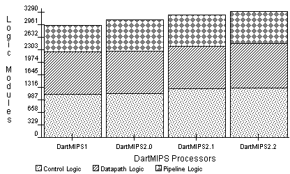
Figure 4
DartMIPS LM Usage by Logic Type
Discussion of Logic Module Utilization
As expected, the logical complexity of our pipelined DartMIPS implementations increased as the design evolved from a simple pipeline to a pipeline with full hazard detection and data forwarding. Most changes were in the control logic; as we expected the pipelined data path changed very little from the sequential DartMIPS1 to the final DartMIPS2.2. In addition the basic control blocks for each pipeline stage remained unchanged, although supplementary logic blocks were required as each new method of resolving hazards was introduced.
Overall, we saw a 12.4% increase in logic from the sequential to the final, pipelined version with forwarding. Of these logic module increases, 48% were due to control logic changes, 38% were due to an increased pipeline register width in all stages to propagate the opcode and some instruction bits (all of which were added with the first pipelined version, DartMIPS2.0), and only 14% were due to data path changes. The changes from DartMIPS2.0 to DartMIPS2.2 are more interesting: there was a 6.7% increase in logic complexity from our simplest to most complex pipelined design; 74% of these changes were in control, while just 22% were in data path and 4% in the pipeline registers.
Design Partitioning
All of our design activity took place assuming we were mapping our design to an infinite chip, an FPGA with infinite logic and I/O resources. Actual implementations of the design must be partitioned: mapped onto an existing set of real FPGA chips.
DartMIPS1 was successfully mapped onto six Actel A1280 devices, with the 2x32x32 register file mapped onto a Xilinx 4005. The 140-pin I/O limit was a serious constraint; only two chips had over 80% LM usage (the other four were under 40%) but the average I/O usage was 91%. In the case of our DartMIPS2 family of pipelined processors, preliminary analysis indicates that versions 2.0 and 2.1 would fit into the same partitioning with 100% I/O utilization on at least two of the chips. 2.2, however, could not be implemented with six A1280's, due to the radically increased I/O brought on by the data forwarding buses. An effort to partition using the virtual wire method of Babb (1993) looks very promising, although an ensuing decrease in performance would be expected.
CONCLUSIONS
The focus of this project was the incremental development of a fully-pipelined, FPGA-based MIPS implementation to serve as an experiment for obtaining quantitative design data. Starting with a sequential version of DartMIPS, we first created a simple pipelined machine and then added functionality for increasingly complex (and higher performance) hazard detection, interlocking, and avoidance. Our most complex design represents only a 12.4% increase in logic module utilization for an expected 30% improvement in CPI (Erickson 1993, Patterson and Hennessy 1993).
We observed that as our design became more complex our verification effort became much more difficult. Part of this activity was regression testing, ensuring that test sets for previous versions, where appropriate, functioned properly on the newest, more complex version. Considerable effort was also expended creating new test sets for the new functionality, which had to be carefully crafted to produce the required test states.
Our experience indicates that the existence of an automatic partitioning tool would greatly assist designers in implementing complex systems on FPGAs. In an ideal design environment, users would target systems for a "virtual" FPGA: one with as many resources as necessary to accommodate the design. This virtual design would then be mapped onto physical FPGAs by CAD software, in much the same way as an operating system maps virtual memory to physical memory. Currently users must be aware of the physical constraints of their target devices from the beginning of the design process. We hope that as FPGA and CAD technology matures, tools for partitioning will become available that will enable users to separate designs from implementation technology.
Finally, we have demonstrated the utility of FPGAs in quantitative analysis of design tradeoffs. A more extensive survey of several systems that explores these issues further is currently in preparation (Fagin et al 1993). Future work includes the examination of more advanced CPU features, such as superscalar processing, a study of other systems besides microprocessors, and a comparison of FPGA-based results with full custom designs. We believe it important to understand how well data obtained with FPGAs generalizes to other technologies.
ACKNOWLEDGEMENTS
This research was performed at the Thayer Rapid Prototyping Facility, a laboratory for the rapid design and evaluation of digital systems. Support for the RPF was generously provided by Actel Corporation, Xilinx Incorporated, Sun Microsystems, National Semiconductor Incorporated, Direct Imaging Incorporated and Hewlett Packard Corporation. Direct support for this research was provided by the National Science Foundation under grant #MIP-9312350. Finally the authors would like to thank Vishal Gupta, Don McManus and Andrei Pascovici for their assistance in the design and testing of DartMIPS.
REFERENCES
Actel Incorporated, ACT Family Field Programmable Gate Array Databook, 1992.
Babb, J., Tessier, R., and Agarwal, A., "Virtual Wires: overcoming pin limitations in FPGA- based logic emulators," Proc. IEEE Workshop on FPGAs for Custom Computing Machines, April 1993.
Erickson, J., McManus, D., Gupta, V., and Pascovici, A., DartMIPS: A MIPS RISC Processor Emulation using Antifuse FPGAs, Thayer School of Engineering, Dartmouth College, March 1993.
Erickson, J. Erickson, J., McManus, D., Gupta, V., and Pascovici, A., DartMIPS2: A Pipelined MIPS RISC Processor Emulation Using Antifuse FPGAs, Thayer School of Engineering, Dartmouth College, June 1993.
Fagin, B. "Quantitative measurements of FPGA utility in special and general purpose processors", Journal of VLSI Signal Processing, 6, pp 129-137, 1993.
Fagin, B., Erickson, J., and Chintrakulchai, P., "Quantitative analysis of RISC processor design tradeoffs using field programmable gate arrays", submitted to IEEE
Transactions on Computers, August 1993.
Hennessy, J. and Patterson, D., Computer Architecture: A Quantitative Approach, San Mateo, CA, Morgan Kaufmann Publishers, Inc., 1990.
Kane, G. and Heinrich, J., MIPS RISC Architecture, Englewood Cliffs, New Jersey, Prentice Hall, Inc., 1992.
Patterson, D. and Hennessy, J., Computer Organization & Design: The Hardware/Software Interface, San Mateo, CA, Morgan Kaufmann Publishers, Inc., 1993.
Xilinx Incorporated, The XC4000 Data Book, 1992.