Rapid Prototyping Without MOSIS: A Minority View
Barry Fagin
Charles Hitchcock
Thayer School of Engineering
Dartmouth College
Hanover, NH 03755
ABSTRACT
There is a widespread consensus in the academic community that MOSIS is an essential part of the rapid prototyping of digital systems. We challenge this view. We describe our experiences with developing a program from the ground up, and discuss how commercial IC-based rapid prototyping can be successfully integrated into an academic environment.
Section 1. Overview
In the fall of 1988, the authors began to review the computer engineering program at Dartmouth College. We believed our program should be centered around the design, implementation, and testing of hardware designs by students. We believe such prototype construction is the most important factor distinguishing computer science from computer engineering.
Like most universities, we considered a VLSI/MOSIS-based system design course, but found this unsatisfactory. The 6-8 week turnaround time from CIF files to chips was poorly suited to Dartmouth's academic schedule, based on 10-week quarters. We felt that the problems of maintaining student enthusiasm and continuity of course content associated with MOSIS made other options more attractive.
We chose instead a commercial IC-based approach, using industrial CAD tools and PCB development products to shorten the design cycle. These products can reduce the turnaround time for the production of a prototype from weeks to days, or even hours. Our efforts have resulted in 1) the Thayer Rapid Prototyping Facility, used for the design and testing of digital systems, and 2) a two-term computer design course sequence.
This paper discusses our experiences with these two aspects of a growing computer engineering program. We discuss our reasons for not choosing MOSIS, our relations with industry, and the delicate balance between teaching and research. We offer suggestions to other faculty interested in developing similar programs, and describe plans for future work.
This paper is divided into eight sections. Section 2 discusses previous work in rapid prototyping. Section 3 gives a brief description of Dartmouth College, the Thayer School of Engineering, and the development of its computer engineering program. Section 4 analyzes the advantages and disadvantages of MOSIS for system design instruction and research. Section 5 introduces the Thayer Rapid Prototyping Facility, while section 6 describes the two-term computer design sequence. Section 7 relates what we have learned from our efforts, and section 8 states our conclusions and plans for future work.
Section 2. Previous Work
Of particular interest to us was the December 1986 Workshop on Rapid Prototyping of Experimental Digital/Analog Systems [Work86] sponsored by NSF and DARPA, and held at Carnegie-Mellon University. This workshop included 27 participants from funding agencies, industry, and (mostly) universities doing systems research.
The final report of the workshop put forward several recommendations:
• The development of courses to help researchers and instructors become more proficient with systems design topics (perhaps in the style of the 1985 summer CMOS instructors course)
• The creation of regional laboratories to enable researchers to build prototypes which would be infeasible using only local facilities.
•Encouraging inter-agency funding of board-level CAD tool purchase for university use.
• Making a PCB design help service available to interested university designers
To our knowledge, none of these recommendations have been implemented.
Currently, many universities do non-MOSIS rapid prototyping. The Microelectronic Systems Lab at the University of North Carolina, for example, does extensive work with printed circuit boards [Ch88]. Students at Indiana University use a custom-designed backboard to implement a complete PDP-8 computer from MSI components [Bo88]. Engineers at the University of Washington Image Processing Systems Laboratory have produced plug-in cards for the IBM AT using MSI and LSI components [Gu88].
Section 3. Computer Engineering at Dartmouth
Last fall, the authors began to restructure the computer engineering program at Dartmouth. Existing offerings lacked continuity and structure, and failed to meet the growing demand for computer engineering courses at the undergraduate and graduate level. A more cohesive program, it was felt, would strengthen the academic offerings of the engineering school. Such a program would also further the professional goals of the authors, who have an obvious interest in creating an environment conducive to computer engineering research.
We designed the program with the following goals in mind:
1) Infrastructure creation.
2) Curriculum development.
3) Accessibility.
4) Accommodation of a wide variety of educational needs.
5) Expanded contacts with industry.
6) Support for research.
7) Production of Actual Prototypes.
We focused our efforts on goal 7, believing that if we could come up with an infrastructure to produce hardware designs in a reasonable amount of time, and develop courses that could use it, we would have the principle features of the desired program in place. Consequently, we turned our attentions to MOSIS.
Section 4. Advantages and Disadvantages of MOSIS
The widespread role of MOSIS in universities is well known [FrPi88], and needs no elaboration here. Many universities, including Dartmouth, have successfully used MOSIS to fabricate student designs reliably and cheaply. We cannot imagine a better support service for our two VLSI design courses.
When choosing technologies for a computer design course, there are several advantages to developing a VLSI-based course and using MOSIS to fab student projects. First, VLSI-based designs can be faster and use less power than comparable designs based on commercial ICs. VLSI student designs also offer higher performance than those produced in a commercial IC-based course. Finally, MOSIS satisfies the "hot hand" syndrome [Ma88]: students get something back for their efforts.
Perhaps the most important advantage, from the point of view of a university, is the issue of cost. MOSIS charges for fabricating student projects are quite low. Prices range from $11,800, for a 7.9 x 9.2 mm die using 2 micron CMOS technology, down to $400 for a 3 micron CMOS TinyChip [FrPi88]. These prices are significantly lower than commercial rates, making MOSIS the only way for many universities to fabricate student VLSI designs.
Using VLSI and MOSIS in a system design course, however, has its drawbacks. For one, there is the difficulty associated with producing functional designs, and correcting mistakes should the designs prove incorrect. As anyone who has taught a VLSI design course knows, obtaining functioning chips for designs of non-trivial complexity is extremely difficult.
The issue of design flexibility is also important. If the chip does not work when it comes back from MOSIS, there is virtually nothing the student can do. Her enthusiasm for the project has in all likelihood evaporated. She would have to be exceptionally motivated to 1) find the problem, 2) fix it, 3) wait for the next MOSIS run, and 4) wait eight weeks for the next design to come back from MOSIS, all while taking a full course load.
This brings us to the most significant disadvantage of MOSIS: the turnaround time between the submission of a design and the return of the chip to the student. Typical times range from six to eight weeks [FrPi88]. This presents several problems in an academic environment, including maintaining continuity, maintaining student enthusiasm, and grading.
Universities on a semester system can address this problem with little difficulty, by scheduling a two semester sequence around the time the chip is fabbed. Universities on a quarter system face a greater challenge. Our current approach is to have students design a simple project during the fall term, with their grade withheld until the project comes back from MOSIS and a final report is written up. A more promising approach, adopted by Charles Seitz at Cal Tech, is to teach a VLSI course sequence that runs through the entire academic year [Ga88]. Small projects are fabricated first, with more advanced VLSI material covered while the projects are being fabricated. Large projects are then fabricated in the winter and spring terms.
This approach is useful for addressing the continuity and idle time problems of a MOSIS-oriented course in a quarter-based academic calendar, but other factors may prevent its adoption. At Dartmouth, for example, the authors would be unable to staff a new three-term course sequence while meeting other teaching obligations. A year-long sequence also represents a formidable course commitment at an interdisciplinary school like Thayer. Such an approach would conflict with our goals of maximum accessibility and the accommodation of students with differing educational and professional goals.
These and other factors led us to reject a VLSI/MOSIS-based approach for our computer engineering courses, and to instead pursue another strategy. Students would design with commercial chips, produce wire-wrapped or printed circuit designs, and debug their projects almost immediately. We thus required institutional support that permitted us to go from blackboard designs to working prototypes in as little time as possible. This resulted in the Thayer Rapid Prototyping Facility.
Section 5. The Thayer RPF
No program can succeed in teaching digital systems design without the institutional infrastructure in place to rapidly produce and evaluate computer designs. For our program, this infrastructure is provided by the Thayer Rapid Prototyping Facility.
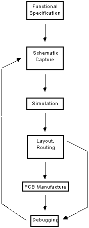
The Thayer RPF is designed to accelerate all stages of the system design process. A simplified view of this process is shown below:
FIGURE 1: The System Design Process
The design begins with functional specification and a high-level block diagram. Hardware components are selected, and the design entered with schematic capture tools. The design is simulated , and a netlist generated. After placement, the design may then be wire-wrapped, producing a prototype immediately, or the netlist may be used as input to a PCB layout program. Layout and routing tools produce a board description file, which can be shipped to a board manufacturer. The resulting board is populated with ICs and tested.
The goals of the Thayer RPF are 1) to have all steps of this process performed in the same laboratory, and 2) to produce working prototypes as quickly as possible. To achieve these goals, we are attempting to construct an integrated environment of commercial products. These products are described below.
5.1 Hardware Platforms
Clearly, CAD tools are required for the rapid prototyping of digital systems. CAD tools, in turn, require hardware platforms to run on. We have chosen the Sun 3/60 as the main workstation for the Thayer RPF. Currently, we have four monochrome stations, and plan to acquire four more color models.
5.2 Design and Simulation Tools
We chose the Workview
® tool package, from Viewlogic Incorporated, to accelerate the schematic capture and simulation stages of the design process. Workview provides a complete schematic capture and simulation package, including back-annotation, hierarchical schematics, an extensive parts library, and support for device modeling. Workview is available at a substantial discount for universities, and interfaces to a wide variety of PCB layout systems.5.3 Placement and Routing
If a wire-wrapped design is to be produced, further CAD assistance is not required. If a printed circuit board is to be developed, however, then more work is necessary.
Currently, we are using the Racal-Redac PCB layout system, running on the IBM PC. This system is quite affordable; at $750, it can be accommodated by most university budgets. However, we would prefer to have schematic capture, simulation, placement, layout, and routing all executed on the same system, so we are examining other Sun-based PCB programs.
5.4 PCB Manufacture
Shipping a Gerber file to a PCB manufacturer and receiving a finished board takes a few weeks, and may even be slower than MOSIS. There are also problems in finding companies willing to handle small quantities within a university budget and time schedule. To address these problems, the Thayer Rapid Prototyping Facility will employ commercial prototyping tools for rapid PCB manufacture.
There are at least three commercial products available for PCB manufacture in the laboratory: the LPKF Circuit Board Plotter, manufactured by CAD/CAM Systems Inc, the IBC BoardMaker, manufactured by Instant Board Circuits Corporation, and the System One, manufactured by PC Proto Inc. The LPKF and IBC products take copper blanks and drill the necessary holes and trace outlines. The System One uses a chemical etching process to produce conducting traces on a flexible plastic film.
These products can produce boards in a matter of hours, or even minutes. Such a short turnaround time of a few hours has several obvious advantages over MOSIS. Students retain more enthusiasm, they get their designs back quicker, and mistakes are more easily corrected.
We note that MOSIS has offered a PCB service to universities. We find this option unattractive for two reasons. For one, the service uses IC mask generation, blown up to generate artwork. This is an unconventional technique, and not supported commercially to our knowledge. Additionally, artwork is expected to be supplied in CIF. Tools that use CIF tend to be IC-oriented, and not well suited to PCB designs.
5.5 Testing
The testing and debugging of complex digital systems requires a sophisticated pattern generator and logic analyzer. Such a system should interface easily with the simulation tools of the CAD system being used, to enable rapid comparison of simulation output vectors with observed output vectors. We are examining a variety of products for the Thayer RPF, including the the HP 16500A and the IMS Logic Master ST.
5.6 Commercial Product Integration in the Thayer RPF
The steps of the design process, together with the commercial tools designed to accelerate each one, are shown below:
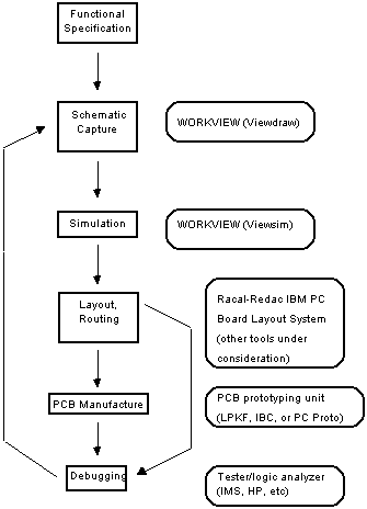
FIGURE 2: Commercial Components of the Thayer RPF
Section 6. Curriculum Development
New courses are a crucial part of any growing computer engineering program. We envisioned the following goals for our new courses:
• Project oriented structure. The courses would be built around student projects. To paraphrase Lynn Conway, computer design is not a spectator sport.
• Maintain continuity. The new courses should be as cohesive as possible. This is a special challenge in a quarter-based academic year.
• Advance research goals. In addition to teaching computer design, we hoped the new courses could assist in our research. Following the advice of Smith [Sm88], we wanted to make sure that our research did not suffer as a consequence of new course development. The classic successful examples of new course development advancing research were the Berkeley CS292x classes, which produced the RISC I microprocessor.
Arguably, the best solution would have been to adopt a three-term course sequence, the approach taken at Cal Tech and elsewhere. Unfortunately, the authors were unable to staff a three-term sequence while meeting other teaching obligations. As a one-term course was too short to permit the debugging and testing of a prototype design, we settled on a two-term sequence. Each of the authors assumed responsibility for one term.
Several lectures in our courses were given by engineers from industry. These engineers have considerable "real world" experience in digital system design, including issues like PCB layout, design for testability, design management, and system testing. We believe industrial engineers have more expertise than professors on a variety of topics, and should be included in any advanced digital design course.
Section 7. What We Have Learned
Currently, we are nearing the end of the first term, and have learned a great deal.
1) Create a well-documented design spec. before the course begins. It is crucial that students not begin designing until the problem is well understood, even if this takes longer than expected. Owing to difficulties in getting the students to master the problem under investigation, we were not able to produce a netlist by the end of the term.
2) Ensure that the students are adequately prepared. Most of our students had difficulty designing a multiplier/divider, a project that we felt was not particularly challenging. Many of our graduate students are from foreign countries, and were not experienced with sophisticated CAD tools. It took them longer to get up to speed than we expected.
3) Workview is an impressive CAD package. Our experience with Workview has been strongly positive. The tools are well documented, easy to use, and conceptually powerful. We have exercised the tools extensively, and have found only one reproducible bug (pertaining to the printing out of schematic files). Thus the software appears to be extremely well tested. So far, we have examined the schematic capture and simulation tools; both have performed well. The interface to the Racal-Redac system also functions correctly.
4) There is a tension between teaching and research.
When trying to teach a course that both educates students and attempts to expose them to research topics, conflicts are inevitable. For example, a course devoted exclusively to teaching well understood concepts should be open to all, in the belief that most people can and should be exposed to the material. A research-oriented course, however, may be better suited to limited enrollment in which students are hand-picked by the instructor.
5) Get a knowledgeable student assistant. We concur with Smith [Sm88], who has commented on the desirability of having good student help to deal with the day-to-day problems that arise in a design course. We are fortunate to have an excellent teaching assistant, who got up to speed with the tools very quickly and produced good documentation to help the other students.
6) Going with commercial IC-based designs was a good decision. While we are somewhat behind schedule, we see no reason to regret our decision to bypass VLSI and MOSIS. We have confidence that we will be able to turn around our designs very quickly, and that students will be quite excited at the prospect of debugging their own designs next term.
It might be argued that by choosing MSI and LSI-based designs, we are designing with yesterday's technology. VLSI has a certain sex appeal: IC masks look good in color, Versatec plots look good on the lab wall, and VLSI circuits offer the highest performance. We can only state that we find correctly functioning LS-TTL computers sexier than malfunctioning VLSI CAMs. We are interested in rapidly evaluating hardware solutions to hard computational problems. We believe that an MSI and LSI-based approach, coupled with sophisticated commercial tools for accelerating the design process, are the best way to achieve this goal.
Section 8. Conclusions
MOSIS is not essential to the rapid prototyping of digital systems. We believe that MOSIS is best suited for VLSI design courses, in which technology-specific principles of VLSI design are to be taught and demonstrated. Universities on a semester system are better poised to handle the six to eight week turnaround time for MOSIS chips than universities on a quarter system. MOSIS would be more attractive for system design courses if the turnaround time were days instead of weeks, but that is asking the impossible of an already impressive service.
An institution doing research in digital system design requires the supporting infrastructure to rapidly produce and evaluate prototypes. This is embodied in the Thayer Rapid Prototyping Facility, a single laboratory equipped with commercial products to accelerate each step of the design process. The capital outlays required for such a facility are nontrivial; industrial sponsorship is all but essential. Currently the Thayer RPF contains workstations, CAD tools, and PCB layout support. Future plans include the acquisition of a Sun-based PCB layout program, a PCB prototyping device, and system test tools.
In addition to building the infrastructure for digital systems research, we have developed two new courses in computer design. Students in these courses design a hardware solution to a computationally intensive problem using the facilities of the Thayer RPF. So far, we have learned that adequate preparation of students is important, and that many of our original goals for the courses conflicted with one another. There is a special challenge in mixing teaching and research.
Section 9. Acknowledgements
We are grateful for the support and understanding of our students in ENGS 199, who endured the inevitable growing pains of an experimental course. We also wish to acknowledge the TA for ENGS 199, Adam Erickson, who has done a superb job in making the course run smoothly. We are pleased to acknowledge support from Viewlogic Incorporated, who made their product available to us at a substantial discount. Finally, funds for the Thayer RPF and curriculum development were provided through startup grants to the authors from the Thayer School of Engineering, without which this work would not have been possible.
The authors can be reached electronically, at barry.fagin@ dartmouth.edu and charles.hitchcock@dartmouth.edu.
Section 10. References
[Bo88] Bouldin, Daniel, "VLSI Curriculum Survey", 1988 VLSI Education Conference and Exposition, Santa Clara Ca.
[Boy88] Boyer, David, Indiana University, personal communication.
[Ch88] Chi, Vernon, University of North Carolina, personal communication.
[FrPi88]Fry, Kathleen and Pina, Cesar, "The MOSIS System", 1988 VLSI Education Conference and Exposition, Santa Clara CA.
[Ga88] Gajski, Daniel et. al. "Migration of VLSI Education Into the Undergraduate Curriculum", 1988 VLSI Education Conference and Exposition, Santa Clara CA.
[Gu88] Guzak, Chris, University of Washington, personal communication.
[Ma88] Maly, Wojciech, "VLSI Education on the Undergraduate Level", 1988 VLSI Education Conference and Exposition, Santa Clara CA.
[PaSe82] Patterson, David and Sequin, Carlo, "A VLSI RISC", Computer, Vol. 15 No. 9, September 1982.
[Sm88] Smith, Michael, "Initiation of a VLSI Teaching and Research Program at the University of Hawaii", 1988 VLSI Education Conference and Exposition, Santa Clara CA.
[Work86] Report of the Workshop on Rapid Prototyping of Experimental Digital/Analog Systems, Fuchs, Henry and Poulton, John, eds., Carnegie-Mellon Univ., Dec. 1986.